Basic Block Diagram of PLC

Figure shows basic block diagram of PLC (Programmable Logic Controller). The CPU of PLC is programmed using a programming terminal usually through personal computers or dedicated HMIs. Basic Modules associated with the CPU are external modules and i/o modules along with bit, byte, word and double word addressable memory locations. 


A PLC is an example of a hard real time system since output results must be produced in response to input conditions within a bounded time. 

11:50 | Posted in , | Read More »

Bidirectional Control of DC Motor using transistor based H-Bridge with single input

Controlling a DC motor in both directions often need a H-Bridge, which is nothing but an arrangement of few transistors. If not by using a single input, atmost two inputs be used to control the motor in both the directions. Otherwise, there are chances for accidential burning of transistors by programming errors. For example, if you accidentally set the transistors 1 and 2 in conducting state, shot-circuit current will flow through both of these transistor making them useless for further operations.
At any instant only one of the cross pairs of transistors can be in conducting state as explained earlier. These two pairs of transistors are responsible for the movement of motor in both directions. When 1 and 2 are on, the motor moves in one direction, on the other hand when 3 and 4 are on, the motor moves into other direction. Not Gate is placed to make sure that the two pairs are never turned on together.
How to lock the motor using a single input? The single input can be provided with 1 or 0 forcing the motor to move in either direction. So locking of motor can not be achieved. However if the pulse of 50% duty cycle is given to the input, then the motor will come to halt. One disadvantage of this approach is that the motor will draw current even in the locking state.
The above circuit has been tested practically!
More to Follow

22:02 | Posted in , , , , | Read More »

RMS Voltage Control Circuit with MOC3021 and BT136


Triac is a power electronic component that conducts in both directions when triggered through gate. Figure below shows a generic working of triac.As it can be seen that at time t1, angle of sinusoid is 45' which means that if we triggered triac at this angle i-e at 45', only shaded blue area will pass through the triac and hence through the load. Observe that shaded blue are has RMS Voltage less than the pure sinusoid. This is the basic principle by which RMS Voltage control is accomplished. Firing needs a small pulse at gate that can be give through microcontroller also. Similarly at firing angle 90' (firing angle is an angle with reference zero crossing at which the triac is triggered using gate pulse) , only red part of sinusoid will pass through the triac giving us the RMS 110V for 220V.


Coutesy of Motrola,Inc

MOC3021 is an optotriac (product of Motorola) that is used for isolation between power and driving circuitry. Note that when C828 on the base is applied voltage>0.7V, optotriac gets triggered. As the triac gets triggered now, the positive or negative voltage (whatever maybe) get pass through the gate of BT136 (triac) and hence triggered it. It should be noted here that by using above arrangement we can control the RMS voltage in both directions. What needs to be taken care of, is the triggering time or firing angle.

There is a need of a zero-crossing detector that will give us the reference for providing delay for desired firing angle. In above example, for firing angle to be 90' for 220V 50Hz AC signal, we need to have a delay of 2.5 ms (t1=2.5ms) right after each zero crossing. Usually MOC3021 is driven through microcontroller, which gives the firing pulse on the basis of interrupt generated by the zero-crossing detector. 

The above circuit is mainly used as a dimmer and is often used speed controlling of AC motor. There are other versions of the above circuits available that caters for the inductive load which will be discussed later.

More to follow!

21:16 | Posted in , , , , | Read More »

JK Flip Flop - Combination of SR and T Flip Flop

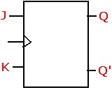
Instead of using a single control input T in T Flip Flop, two inputs J and K can be used instead such that D=JK'+J'K. This kind of flip flop is a beautiful combination of RS Flip Flop and T Flip Flop. 
  • Behaves as RS Latch / Flip Flop (here J=S and K=R) for all input values except for J=K=1
  • For J=K=1, (this is state has to be avoided in SR), JK Flip Flop toggles the value similar to T-Flip Flop.

12:46 | Posted in , , | Read More »

T Flip-Flop using D Flip-Flop

Toggle Flip Flop or T Flip-Flop is interesting representation of modified D Flip Flop. Just by having a feedback, D Flip-Flop can be converted to T Flip-Flop. The modification is given below:
The feedback connections make the input signal D equal the value of Q or Q' controlled by an input signal D. At every positive edge when T=0, D=Q and this state will remain same. When T=1 at positive edge clock, D=Q' and will remain unchanged. The overall operation is that: it retains it present state at T=0 and toggles it when T=1.
Basic application of T-flip-flop is a counter circuit.

12:34 | Posted in , , | Read More »

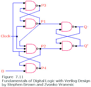
Positive Edge D Flip Flop using 6 NAND gates only

Refer to Master Slave Negative Edge D Flip-flop before you read the next paragraph.
The previously explained circuit was negative edge triggered. The same can be changed into positive edge flipflop by just giving the clock directly to the slave and the complement of it to master. However there is another circuit that accomplishes the same task and requires only 6 NAND gates means fewer transistors and efficient design.

How the above circuit works? ....explained below:
  • When clock=0, P1 and P2 are high (i-e P1=P2=1). keeping the values of Q and Q' intact. 
  • At the same time P4= complement of D and P3=D.
  • Now when clock=1 (at positive edge), the values of P3 (equal D) and P4 (complement of D) passes through P1 and P2.
  • Now P1=D' and P2=D which means Q=D and Q'=D'
It is also necessary that while clock=1, D must be in don't-care state. Two cases (when clock=1) needs to be studied:
  • When D=0, P2=0 which will keep the value of P4=1 regardless of the value of D
  • When D=1, P2 and P3 remains high regardless of the value of D.
This implies that the above flip-flop ignores the changes in D when clock=1 (i-e after positive edge of the clock)

12:12 | Posted in , , | Read More »

Working of Master Slave Negative Edge D Flip-Flop

Latches were level sensitive; means the state of latch gets change according the values of input signal only when the clock is active. But practically there is often need to have a storage elements that can change their state only once during a clock cycle. Flipflop fall under this category. Master Slave and D Flipflop are the two basic types of flipflops. 

As seen in the figure, Master-Slave D Flip-flop consists of two D Latches. Master changes its state when clock=1 while the latter changes its state when clock=0. When the clock is high the masters track the value of D but since the slave is in inactive state, Qs also remains unchanged, Now when the clock signal goes low, the master goes to inactive state and the slave which is now in active state it tracks the value of Qm. While clock=0, Qm does not change its value. Thus we can say that only once during the clock cycle the slave can undergo change in its value. This gives us a generic idea of working of flip-flops.

It can also be observed that only during the transition from 1 to 0, the output gets change. This transition is referred to as "an edge". Transition from 1-0 is termed as negative edge while in the opposite case it is called positive edge. In this particular case our flip-flop is negative edge triggered. Bubble with arrow indicates that the flipflop is negative edge triggered. 

More to follow

11:00 | Posted in , , | Read More »

Gated SR Latch using NAND Gates

Gated RS Latch can also be formed using NAND gates only in a cross-coupled fashion.  The behavior of the circuit is the same as was explained previously. (See Gated SR Latch using NOR Gates). This gate is usually preferred over others because it requires fewer transistor than was required to make the same gate using AND gates. Characteristic Table along with the symbol can be found below:

12:29 | Posted in , , | Read More »

Gated SR Latch using NOR Gates

Previously explained was a simple SR Latch that was holding its last states on specific input. Often there is a need to enable or disable a latch. To accomplish the same we need to have an extra input pin called clock for enabling or disabling the latch. When disabled, the previous states remain unchanged. Circuit that uses this type of mechanism are called gated latches. In this case the circuit is called Gated SR Latch.

This latch is active high, that is when clock signal goes high the Gates SR Latch behaves as a normal SR Latch. And when the clock signal goes low, whatever the logic at inputs maybe, the output will remain the same unless and until the clock signal goes high again.


The characteristic table is given below. Many authors use the term characteristic table rather than truth table - this is because truth table is usually linked with the circuits whose output(s) solely depends upon the input(s) only which is not the case here. The table below is same as that of SR Latch except that it is controlled using clock signal.

12:14 | Posted in , , | Read More »

A Memory Element using NOR Gate - SR Latch


A memory element is referred to as a storage element. A basic memory element can formed using NAND or NOR gate. The above arrangement of NOR gate is a basic memory element that can withhold a logic. The arrangement below is a modified version which is also known as SR Latch. 

Summarization of mentioned characteristic table for above SR latch is given below :
  1. When Q=0, Q'=1 and when Q=1,Q'=0 under normal conditions
  2. When R=0 and S=1, the latch is set into "S E T" state i-e Q=1 and Q'=0
  3. When R=1 and S=0, the latch is set into "R E S E T" state i-e Q=0 and Q'=1
  4. When both R and S equals low logic, the SR latch holds is previous states
  5. The last possibility of R=S=1 gives us the illegal (unpredictable|) value. Some authors say that Q=Q'=0 in this state.
More to Follow

09:39 | Posted in , , | Read More »

Block Diagram of Ethernet Based Control of Electric Appliances with Touch Panel Interface


The above block-diagram shows a model of Ethernet automation. The same phenomenon is equally applicable for industrial Ethernet with some amendments.  Also the above block diagram is point-point link approach only. The same can be extended to layer-2 network for more sophisticated automation.

What's happening in the block diagram? Touch Screen is placed at user end, say in a control room. Attached with it is a touch screen controller which get the coordinates of touch screen and pass over to Ethernet module. Ethernet module consists of a microcontroller, an Ethernet controller and Ethernet link. Microcontroller on the basis of received coordinates will pass the instructions to Ethernet Controller (ENC-28J60) over SPI. Ethernet controller will then transmit control words / data to its counterpart at the other end. Microcontroller will then drive the triac based or whatever the circuitry maybe accordingly.

More to follow!

11:19 | Posted in | Read More »

Block Diagram of DC Servo System


What is a Servo Motor? A servo motor comprises of mostly DC motors with feedback for position controlling. Stepper motor is also used for position controlling but without feedback. Mostly Servo Motors are DC because they provide high locking power. The above block diagram depicts the basic block diagram that most of the servo systems are based on. Microcontroller  provides PWM signal to the H-Bridge which onwards drive the motor in either direction on the basis of received input PWM signal. Lets say if PWM signal of 50% duty cycle locks the motor, so increasing or decreasing PWM value will drive the motor in CW or CCW direction. The Shaft of the motor is connected to potentiometer thus changing the Vf ( Feedback Voltage) as the motor rotates. User can set the desired position of the motor using another potentio meter. This is the Set-point voltage. Microcontroller takes the difference of both the voltages i-e Feedback and Set-point and generates a PWM signal such that Motor reaches the desired position. When it does do, the difference gets zero and ultimately motor comes into locking position. This is how DC motor servo system operates. More to Follow!

13:08 | Posted in , , | Read More »

MATLAB based Project Ideas

Taken from http://www.home.agilent.com
MATLAB is high level technical computing language that is serving as primary tool in major projects especially those concerning with Image Processing, Medical Imaging and Digital Signal Processing. Simulink is also one of the product of MATLAB. Developing algorithms, Analyzing and visualization of have become far easier and faster. Mathworks claims that MATLAB is even faster than traditional programming languages like C,C++ and JAVA. 


Here is list of project ideas based on MATLAB for graduate and post-graduate students:

  1. Impulse Noise Filter
  2. Palm-print identification system
  3. Finger-print identification system (enhancement using filtering)
  4. Modelling of 3-phase power system (Filtering method)
  5. Implementation of Motion detection algorithm
  6. Digital Filter (Bilateral) for image diffusion
  7. Code Shift Keying Impulse Modulation
  8. Speaker Recognition in Noisy Environment
  9. Principal Component Analysis for face recognition
  10. Designing Antenna using CDMA
  11. Voice Recognition
  12. Coding of Stereoscopic Images
  13. Touch less Finger Print recognition system
  14. Ultrasound Speckle Image Processing
  15. Development of Sesmographic system
  16. Analysis of Volumetric Chest CT Scans
  17. Bit Error Rate Analysis of OSTBC Transmission
  18. Text independent speaker verification
  19. Iris recognition algorithm
  20. Online Signature verification algorithm
More to follow!

22:23 | Posted in , | Read More »

Basic Block Diagram of Data Acquisition System (DAS)

Data Acquisition System is an important subject having its vast applications specially in industries. Often Data Acquisition System is abbreviated as DAS or DAQ. The process that most of the Data Acquisition System follows is to sample the data that represents real time conditions and to convert it in digital form that computers and processors can manipulate it.

The basic Block Diagram of DAS (Data Acquisition System) can be seen below :


                                    Rights Reserved : http://elprojects.blogspot.com

The data from sensors is fed into ADC for mapping it to digital form. Typical ADC consists of a Sampler, a Quantizer and an encoder. The selection criterion of ADC is an other subject that needs another dedicated post. The data taken from ADC is then fed into microprocessor or microcontroller for the operations like memory or internet provision for remote accessing.

Few of the reasons for the emergence of DAS to digitally acquire data and for Analog Obsoleteness are as under:
  • No processing can be done
  • More memory needed
  • Less readable due to Infinite Readings

12:58 | Posted in | Read More »

Temperature Sensors Comparisons

A number of Temperature Sensors / Heat Detectors are available in the market. Some of them includes:


All of the aforementioned have their own advantages and disadvantages. The pros and cons of each of the following are summarized below in a nutshell:

THERMISTOR:
This device offers the benefit of a very high sensitivity for a range of temperatures but has a non-linear scale. Extensive mathematical calculations are required to cater for this nonlinearity. The benefit is that it is very cheap compared to others. Normally used to detect a threshold temperature and used where accuracy is not needed.

THERMOCOUPLE:
The major advantage that a thermocouple offers to us is the Temperature range. It can be used for a very wide range of temperatures but at the same time it is highly insensitive. Dedicated linearize-rs like AD594( for J-Type - Temp range: 1800'C) and AD595 ( for K-Type - Temp range: 1200'C) are used compensation / amplification / linearization purposes.

DIODE AS TEMPERATURE SENSOR:
The diode is an extremely low cost device but has the disadvantage of a non-linear scale and rates poorly on the reliability scale.

RTD:
Resistor Temperature Device gives linear change in voltage with temperature. Famous of them are PT100 and PT1000. It also has a range that is suitable for normal laboratory and typical applications like fire alarm system. The cost of the RTD sensor is also less compared to thermocouple. 

Solid State temperature sensor that gives linear response. Often there is no need to connect ADC. Range is also suitable for most applications. For more details see LM34/LM35/LM334/LM335 Selection Guide.

11:43 | Posted in , | Read More »

Theory of 8051/AT89S52 based SMOKE DETECTOR and FIRE ALARM SYSTEM

OVERALL THEORY OF THE PROJECT
Report and Coding of above project can be found here.
The project over all consist of the following components:
1.   Microcontroller ATMEL 89S52.
2.   Temperature sensor LM-35.
3.   Smoke sensor TGS-308.
4.   16x2 LCD.
5.   Operational amplifier IC LM-324.
6.   12 Volts Buzzer.
7.   6 Volts Relay.
8.   Potentiometers 10K.
9.   5 Volts Voltage regulator 7805.
10. BJT C-1383 NPN-type
11. Crystal oscillator 11.0592 Mhz.
12. LED’s.
13. Push button.
14. Capacitors.
15. DB-25 Connector.
16. ISP Programmer.
17. KEIL UVision-2.
18. 9 Volts Adapter.
19. Weiroboard.
20. Wiring and miscellaneous.


             Step wise execution of the project is very necessary to fulfill the task. For this purpose first of all selection and purchase of all the components was done. Then the project was first designed on a breadboard. For this purpose first the microcontroller was connected with the crystal oscillator that produces 11.0592 MHz frequency to drive the microcontroller and to provide the clock frequency. After successful production of the frequency fixed 5 volts supply for the microcontroller was to be designed for which voltage regulator 7805 was used with capacitors circuitry. Output of the regulator was fed into the microcontroller’s Vcc. Until this task which is common for every microcontroller based project everything worked all well and fine. Coming to the main stream now the heat sensor LM-35 was interfaced with a comparator that gives an output voltage level for certain temperature. According to the fire environment the output of the heat sensor compares 0.5 Volts DC already set on the comparator IC, hence any increase in the temperature correspondingly increases the output of the sensor and hence the comparator IC was generating the high output thereby giving positive indication of fire.

            
            Similarly smoke sensor TGS-308 was interfaced with the comparator. As the sensor gives certain voltage level upon positive detection of smoke so the comparator was fed with 3 Volts DC to compare with the output of the smoke sensor, as soon as the output of the smoke sensor increases beyond 3 Volts the comparator passes high logic on its output hence indicating positive presence of smoke.


            The output of both these sensors is fed into the microcontroller through pins 2.0 and 2.2. The microcontroller continuously examines these pins and performs AND operation and high output of the AND operation confirms fire, there by sending the operation condition to the buzzer and displaying the location of fire on the LCD through parallel connections through port 1.


            Similarly three more smoke and heat sensors’ output were also being fed into the microcontroller which deals these inputs similarly like the one stated above and hence alarming the buzzer as an output and displaying the presence and the location of the fire on LCD display. Hence giving us a flexibility to interface various sensors at a time with the microcontroller and displaying the exact location of the fire. The output current of the microcontroller is very low, as low as a few microamperes, so buzzer can not be directly driven by the microcontroller as the buzzer must need at least a few milliamperes to sound efficiently and loudly. For this purpose need for a relay to be used was felt that was energized on logic high reception from the microcontroller and in turn was activating the buzzer. Continuous examining of the respective pins of the sensors makes this project highly useful to be used in sensitive and high risk areas.


            Programming of the project needs continuous examining of the pins connected to the output of the sensors and on positive indication sending data to LCD indicating the position of the fire and sounding of the alarm.


More Details see Project Report and Coding

10:25 | Posted in , | Read More »

8051/AT89S52 based SMOKE DETECTOR and FIRE ALARM SYSTEM

Download Project Report


8051 BASED FIRE ALARM SYSTEM
ownership

We, Mr. Hasban Mehmood, S/LT Arslan, S/LT Tauseef and S/LT Sikandar, bearing ROLL/P No. El-614, 7400, 7407, 7410 respectively of national university of science and technology, take an oath and state that the project FIRE ALARM SYSTEM is entirely and devotedly made by us. Previously stated project is owned by us and bears no belonging to anybody else. All the work and efforts in this project has been done only and only by the above mentioned group members. All the work from selection of project to the completion has been done by ourselves, although we have referred to some seniors and instructors of electronics department whenever we faced some problems which happened very often. 


Importance
In any modern structure or building of the world, safety has the highest priority and therefore fire detection system is one of the basic components of the structure. Timely information of fire not only helps save lives but also makes it easier to put out fire. 

Objectives: 
Our objective is to design a Fire Alarm System that would fulfill the following objectives:    
 
  • Indicate the room in which fire erupted
  • Sound the alarm if fire occurs
  •  False Alarm occurrence should be kept minimum
  •  The system should be flexible enough to be easily modified in case if new rooms are added to the building
  •  The system should also provide the flexibility to adjust the temperature and smoke sensitivity levels as per the operating environment
  • The system should never be in any ambiguous state. Under normal conditions the system should indicate the state of the room as ‘NORMAL’ in order to avoid any confusion.

REASONS FOR CHOOSING DIGITAL SOLUTION:
Conventional fire alarm systems having hard wire layout and normally opened warning devices like heat detector and smoke detector in general specifications, have a good view in low price, but have a bad view in

1. Low efficiency to warn and to communicate to human
2. Difficulty of maintenance
3. Hard expansion and transformation of working
4. No record and no database to develop in the future

Our proposed fire alarm system is designed and built to solve these problems. The connections between warning devices are dealt with microcontroller.

GENERAL WORKING OF THE PROPOSED SYSTEM:
This paper proposes the design and construction of fire alarm system which is controlled by 89S52 microcontroller. LCD is used to indicate situations of the system composed of 2 modes of working state, regular working mode and fire mode. Graphic output states are displayed on LCD by using software ‘Keil uVision2’, interfacing with microcontroller. Input signal coming from the normally opened warning devices such as heat detector and smoke detector is sent into a detectable instrument to separate the mode of working state. After that, output signal is dispatched to 89S52 microcontroller for analysis. This microcontroller can transfer data and display the situation of detector in 4 zones. Thus, the environment of the zones is exposed on LCD. In case of fire mode, the data will be sent to LCD and to Buzzer simultaneously.

HOW I WILL GO ABOUT IMPLEMENTING MY SOLUTION:
To make our lives easier and to make maximum use of time available to us, we plan to use the modular design concept to implement our system. The entire system is to be divided into different modules, which not only makes troubleshooting easier but is also an effective approach for system modification.

Our system will consist of the following modules:
HEAT DETECTION CIRCUIT
• SMOKE DETECTION CIRCUIT
• MICROCONTROLLER PROGRAMMING
• INTERFACING OF BUZZER
• LCD INTERFACING

We first plan to implement each of our modules on breadboard. Once the circuit starts to function properly on the breadboard it will be implemented on the weiroboard. In the next step all these modules will be linked together via microcontroller. The software will then be embedded onto the hardware to perform the desired control operations.


HEAT DETECTION CIRCUIT:
This is the first module of our project in which we have used LM 35 sensor and a comparator. LM 35 has three pins a, b and c. Pin a is connected to Vcc, pin b is connected with ground while the output is from pin c .The output of this sensor is going to a comparator .As per our requirement we need to send a high signal to the microcontroller when the temperature is 50 degree centigrade As the output of sensor gives 10mv change with a change of 1 degree centigrade in temperature . So at 50 degree centigrade it will give 0.5 volts as output has a linear relationship with temperature .so to meet our requirement we have set 0.49 volts on the negative input of comparator so that when the output of sensor will give 0.5 volts the comparator will pass high signal to microcontroller. So when the temperature of external environment will be 50 degree centigrade, a high signal will be passed on to the microcontroller through comparator.

SMOKE DETECTION CIRCUIT:
The second module of our project is to detect smoke from the environment which is inevitable outcome of fire. So to fulfill this requirement we have used smoke sensor TGS 308 and a comparator. The sensor output is almost zero when there is no smoke in environment .On the contrary when there is a smoke the sensor will give a output voltage according to the intensity of smoke .As soon as the smoke vanishes its output again comes to zero .The internal circuitry of TGS-308 contains a heater .as the smoke particles will pass through , the heater will ionize the smoke particles and they will act as a charge carriers so a voltage will be built at output .TGS-308 has four pins Pin A, B, C and D. out of these A and B are connected to Vcc, pin D is connected with ground and pin C is the output pin. The output pin is connected with the positive input of comparator while at its negative input there is constant 3 volts .so as the smoke will produce, there will be voltage at output of sensor. As the smoke intensity increase and the sensor output will reach 3.1 volts the comparator will pass a high signal to microcontroller. As this sensor is quite sensitive to smoke so we have kept 3 volts as a standard at comparator input so that it should detect real fire and do not activate on fake signals just like if someone is smoking.

MICROCONTROLLER PROGRAMMING AND INTERFACING:
We have used 89S52 microcontroller. It has 40 pins .pin no 40 is connected to Vcc while pin no 20 with ground. 

LCD INTERFACING:
The LCD we used was having 16 pins out of which 8 pins are directly going to microcontroller pin number 1 to 8. Two pins are connected with Vcc one with ground and one with the potentiometer to set the resolution of LCD. Three control pins of LCD are also connected to microcontroller pin no 2.5, 2.6, and 2.7 .They are used for enabling LCD, performing read or write operations and to select command or data register .

BUZZER:
It has two pins; one is connected with the supply and the other one with the microcontroller pin no 2.4. When microcontroller will provide low signal, the circuit will be completed and the buzzer will start alarming.

SOFTWARE DESIGN
CONDITIONS:
  • In case if both the bits of a particular room are high (i.e. the smoke and heat levels are above  
    normal conditions), the program sets the pin connected to the buzzer, turning it ON. 
    Simultaneously the LCD displays the room number of the room where fire has erupted. 
  • In case if one of the bits of a particular room is set (i.e. either the smoke sensor or h
    is operating above normal conditions), the program takes this situation as ambiguous and  displays “NORMAL” on the LCD.

  • If both the bits are at low logic levels (i.e. both the heat and smoke sensors are operating under normal conditions), the program simply displays “NORMAL” on the LCD and the buzzer also remains OFF.
  • The programming approach to display output on the LCD includes character by character transfer of the entire string with an appropriate delay. The LCD is initialized only once and only the top line of the LCD is being used for display purpose.
SOURCE CODE:

;********************************************************************

 LCD_RS    BIT     P2.7
 LCD_RW    BIT     P2.6
 LCD_EN    BIT     P2.5

 LCD       EQU     P1


;********************************************************************
ORG     000H
      
        CALL    INIT_LCD


again:
        CALL    GET_SENSOR_DATA
       
        MOV               A,#81H  
                CALL        WR_LCD_COMMAND
                CALL DELAY

                JNC HERE
                MOV       A,#' '
                CALL        WR_LCD_CHR
                MOV       A,#'F'
                CALL        WR_LCD_CHR
                MOV       A,#'I'
                CALL        WR_LCD_CHR
                MOV       A,#'R'
                CALL        WR_LCD_CHR
                MOV       A,#'E'
                CALL        WR_LCD_CHR
                MOV       A,#' '
                CALL        WR_LCD_CHR
                MOV       A,#'A'
                CALL        WR_LCD_CHR
                MOV       A,#'L'
                CALL        WR_LCD_CHR
                MOV       A,#'A'
                CALL        WR_LCD_CHR
                MOV       A,#'R'
                CALL        WR_LCD_CHR
                MOV       A,#'M'
                CALL        WR_LCD_CHR
                MOV       A,#' '
                CALL        WR_LCD_CHR
                MOV       A,#'#'
                CALL        WR_LCD_CHR
                MOV       A,#' '
                CALL        WR_LCD_CHR
       
        CLR     P2.4

       
        MOV               A,#31H
                CALL        WR_LCD_CHR

        JMP    AGAIN

HERE:   MOV          A,#' '
                CALL        WR_LCD_CHR
                MOV       A,#' '
                CALL        WR_LCD_CHR
                MOV       A,#' '
                CALL        WR_LCD_CHR
                MOV       A,#' '
                CALL        WR_LCD_CHR
                MOV       A,#'N'
                CALL        WR_LCD_CHR
                MOV       A,#'O'
                CALL        WR_LCD_CHR
                MOV       A,#'R'
                CALL        WR_LCD_CHR
                MOV       A,#'M'
                CALL        WR_LCD_CHR
                MOV       A,#'A'
                CALL        WR_LCD_CHR
                MOV       A,#'L'
                CALL        WR_LCD_CHR
                MOV       A,#' '
                CALL        WR_LCD_CHR
                MOV       A,#' '
                CALL        WR_LCD_CHR
                MOV       A,#' '
                CALL        WR_LCD_CHR
                MOV       A,#' '
                CALL        WR_LCD_CHR
                MOV       A,#' '
                CALL        WR_LCD_CHR

        SETB    P2.4
              
        JMP AGAIN

;************************************************************************

INIT_LCD:
        MOV      A,#38H                ;2 line 5x7
        CALL    WR_LCD_COMMAND   
        MOV      A,#0CH                ;LCD on cursor on
        CALL    WR_LCD_COMMAND
        MOV      A,#01H                ;clear LCD
        CALL    WR_LCD_COMMAND
        MOV      A,#06H                ;shift cursor right
        CALL    WR_LCD_COMMAND
DISP:       MOV       A, #81H  ; Curser at LINE # 1, Position # 3
                CALL        WR_LCD_COMMAND
RET

;**************************************************************************

WR_LCD_COMMAND:
                CALL DELAY
                MOV  LCD,A
        CLR  LCD_RS
        CLR  LCD_RW
        SETB LCD_EN
        CLR  LCD_EN
RET

;***************************************************************************
WR_LCD_CHR:
                CALL DELAY
                MOV  LCD,A
        SETB LCD_RS
        CLR  LCD_RW
        SETB LCD_EN
        CLR  LCD_EN
        
RET
;***************************************************************************
DELAY:
                mov        r5, #0ffh                 ; delay loop instead of checking bit-7
                djnz        r5, $
RET
;****************************************************************************
GET_SENSOR_DATA:

        MOV C, P2.0
        ANL C, P2.2
RET
END

Feel free to contact us at elprojects@ymail.com.

20:49 | Posted in , | Read More »

Labels

Recently Commented

Recently Added