Firstly, what do we mean by digital modulation? Typically the objective of a digital communication system is to transport digital data between two or more nodes. In radio communications this is usually achieved by adjusting a physical characteristic of a sinusoidal carrier, either the frequency, phase, amplitude. This is performed in real systems with a modulator at the transmitting end to impose the physical change to the carrier and a demodulator at the receiving end to detect the resultant modulation on reception. We begin our discussion by three basic types of digital modulations:
- ASK [Amplitude Shift Keying]
- FSK [Frequency Shift Keying]
- PSK [Phase Shift Keying]
All of these techniques vary the parameter of a sinosoid to represent the information we wish to transmit.
A sinusoid has three parameters that can be varied, these are amplitude ,phase and frequency.
- In FSK we change the frequency in response to information. One particular frequency for ‘1’ and another frequency for ‘0’.

- In PSK, we change the phase of carrier signal to indicate information.

23:56 |
Posted in
BASIC ELECTRONICS,
Communication Basics,
Digital Communication System,
Digital Modulation,
How Stuff Works?
|
Read More »
It is necessary to follow some steps inorder to implement asynchronous transmission on PIC microcontrollers. And these steps are summarized below:
- Initialize the SPBRG register for the appropriate baud rate. In the case high speed baud rate is rquired, set bit BRGH.
- Dont forget to enable the asynchronous serial port by clearing bit SYNC and setting bit SPEN.
- For interrupt based transmission enable bit TXIE.
- For 9-bit transmission is desired, then set transmit bit TX9.
- Enable the transmission by setting bit TXEN, which will also set bit TXIF.
- If 9-bit transmission is selected, the ninth bit should be loaded in bit TX9D.
- Load data to the TXREG register (starts transmission). It is to be noted, transmission starts immediately after TXREG is loaded.
- If using interrupts, ensure that GIE bit and PEIE bit (bits 7 and 6 of the INTCON register) are set.
Details to follow!
16:30 |
Posted in
BASIC ELECTRONICS,
Electronics Projects,
PIC,
PIC Microcontroller USART,
USART,
USART on PIC
|
Read More »
PCB designing is usually done on the very popular E-CAD software called OrCAD. Imagine a circuit like that of Ethernet kit using ENC28J60 that has different voltage level such as Low-voltage (3.3V), TTL/CMOS voltage level (5V) and the LAN standard signals levels. It also has the high frequency signals of SPI interface with clock of 10MHz and the LAN standard signals with modulation rate of 20MHz. All these signals may interfere with each other if the tracks of the PCB are not properly routed and the components are not placed to appropriate location due to EMI, this interference may cause the malfunctioning of the circuit. Some rules should be followed to avoid the EMI problems
- Keep the tracks length as short as possible
- Do not route the analog signal and the digital signal together
- Keep the clock track separate from the other signal
- Keep the high frequency signals tracks separate from the other signals.
- Keep the Ground track as short as possible.
- Keep the lengths of the connector short of high frequency signals such as SPI clock (!important)
- Do not turn the route at 90o.
- Never run the clock signal tracks to outer edge of the PCB
- No unrelated component should be closer than 1 inch to the crystal
- Put the crystal not farther than 1 cm form oscillator pin
- Put RBIAS resistor as close as possible to pin.
16:22 |
Posted in
BASIC ELECTRONICS,
How to handle EMI problem in PCB Designing,
PCB Designing Rules
|
Read More »
Here is how the resistive touch screen looks like. A transparent screen having four wires coming out of it for its interfacing. Though transparent, but consists of 2 resistive layers lying parallel to each other one above the other having an air gap (a kind of insulation) in between. What happens is, that when the user touches the touch screen, the two resistive layers gets connected and a voltage divider resistive network is established. Here is the pictorial view of how the resistive network is established.

Now, we need to know the location, where the user have interrupted the touch screen. In order to know that, we will have to calculate the co-ordinates. To calculate the coordinates on the touch screen where the user has touched, we play with four wires coming out of the touch screen. The two wires indicating the x-axis and the other two indicating the y axis. (x and y axis here are the relative directions. So, after the formation of a potential divider network, we apply voltages to X+ and X- and making Y+ OR Y- as a probe (means we take voltages from Y+ or Y-), in the same fashion we take voltage from the X+ or X-. These two voltages we get are function of the resistance which will vary through out as you move in the touch screen.
Now, the two analog voltages you get are fed to the adc for its digitization. What is left now is the mapping of the touch screen as per the requirements. How to interface resistive touch screen with the microcontroller using resistive touch screen controller will be discussed later.
More to follow!
11:38 |
Posted in
4 wire resistive touch screen,
BASIC ELECTRONICS,
How Stuff Works?,
Touch Screen Types
|
Read More »
The basic building blocks involved in digital communication system can be seen in the figure. Some block shown above might seem strange for the newbies. Source Coding is the process of compressing the data efficiently. In other words, source coding is the process of optimizing the length of data. An example of this can be a surveillance system. It is useless to send the whole background of the image when a motion is detected. Source coding is thereby used to send only that portion of a frame which is being changed and not the useless information in terms of the whole background. Another example of this could be the transmission of English Text. We know that the probability of occurrence of vowels i-e a,e,i,o,u is more than the other alphabets thereby giving a clue to compress the English Text in terms of bits transmitted.
After that comes the Channel Coding. For a layman, it can be referred to as opposite of Source Coding in term of process. Channel coding involves the addition of redundant bits to a message signal that will make up for the errors. This involves the identification and as well as the correction of errors, if any. Hamming code it the best example of Channel Coding. Modulation and Demodulation needs another post for discussion which will be discussed later.
More to Follow!!
18:01 |
Posted in
BASIC ELECTRONICS,
Block Diagrams,
Digital Communication System
|
Read More »
LM34 and LM35 are solid state temperature sensors that are most widely used in the laboratories and often deployed in appliances used in offices and houses. Before you select LM34 or LM35 as your temperature, you must have a fair idea about the the selection criterion of both the ICs. You can read Selection Criterion of LM34 and LM35 which compares the basic properties of both the ICs in way that is easier to understand. LM35 and LM34 gives 10mV/C and 10mV/F respectively. The electrical characteristic can be seen from the datasheet of National Semiconductor which you can also download from below.
17:07 |
Posted in
BASIC ELECTRONICS,
Datasheet,
Downloads,
LM34,
LM35
|
Read More »
Figure shows basic block diagram of PLC (Programmable Logic Controller). The CPU of PLC is programmed using a programming terminal usually through personal computers or dedicated HMIs. Basic Modules associated with the CPU are external modules and i/o modules along with bit, byte, word and double word addressable memory locations.
A PLC is an example of a hard real time system since output results must be produced in response to input conditions within a bounded time.
11:50 |
Posted in
BASIC ELECTRONICS,
Block Diagrams
|
Read More »
Controlling a DC motor in both directions often need a H-Bridge, which is nothing but an arrangement of few transistors. If not by using a single input, atmost two inputs be used to control the motor in both the directions. Otherwise, there are chances for accidential burning of transistors by programming errors. For example, if you accidentally set the transistors 1 and 2 in conducting state, shot-circuit current will flow through both of these transistor making them useless for further operations.
At any instant only one of the cross pairs of transistors can be in conducting state as explained earlier. These two pairs of transistors are responsible for the movement of motor in both directions. When 1 and 2 are on, the motor moves in one direction, on the other hand when 3 and 4 are on, the motor moves into other direction. Not Gate is placed to make sure that the two pairs are never turned on together.
How to lock the motor using a single input? The single input can be provided with 1 or 0 forcing the motor to move in either direction. So locking of motor can not be achieved. However if the pulse of 50% duty cycle is given to the input, then the motor will come to halt. One disadvantage of this approach is that the motor will draw current even in the locking state.
The above circuit has been tested practically!
More to Follow
22:02 |
Posted in
BASIC ELECTRONICS,
Electronics Circuits,
H-Bridge,
H-Bridge with single input,
How Stuff Works?
|
Read More »
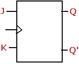
Instead of using a single control input T in T Flip Flop, two inputs J and K can be used instead such that D=JK'+J'K. This kind of flip flop is a beautiful combination of RS Flip Flop and T Flip Flop. - Behaves as RS Latch / Flip Flop (here J=S and K=R) for all input values except for J=K=1
- For J=K=1, (this is state has to be avoided in SR), JK Flip Flop toggles the value similar to T-Flip Flop.
12:46 |
Posted in
BASIC ELECTRONICS,
Digital Electronics,
JK Flip Flop
|
Read More »
Toggle Flip Flop or T Flip-Flop is interesting representation of modified D Flip Flop. Just by having a feedback, D Flip-Flop can be converted to T Flip-Flop. The modification is given below:  The feedback connections make the input signal D equal the value of Q or Q' controlled by an input signal D. At every positive edge when T=0, D=Q and this state will remain same. When T=1 at positive edge clock, D=Q' and will remain unchanged. The overall operation is that: it retains it present state at T=0 and toggles it when T=1.
Basic application of T-flip-flop is a counter circuit.
12:34 |
Posted in
BASIC ELECTRONICS,
Digital Electronics,
T-Flip Flop using D Flip-Flop
|
Read More »
Refer to Master Slave Negative Edge D Flip-flop before you read the next paragraph.
The previously explained circuit was negative edge triggered. The same can be changed into positive edge flipflop by just giving the clock directly to the slave and the complement of it to master. However there is another circuit that accomplishes the same task and requires only 6 NAND gates means fewer transistors and efficient design.
How the above circuit works? ....explained below:

- When clock=0, P1 and P2 are high (i-e P1=P2=1). keeping the values of Q and Q' intact.
- At the same time P4= complement of D and P3=D.
- Now when clock=1 (at positive edge), the values of P3 (equal D) and P4 (complement of D) passes through P1 and P2.
- Now P1=D' and P2=D which means Q=D and Q'=D'
It is also necessary that while clock=1, D must be in don't-care state. Two cases (when clock=1) needs to be studied:
- When D=0, P2=0 which will keep the value of P4=1 regardless of the value of D
- When D=1, P2 and P3 remains high regardless of the value of D.
This implies that the above flip-flop ignores the changes in D when clock=1 (i-e after positive edge of the clock)
12:12 |
Posted in
BASIC ELECTRONICS,
Digital Electronics,
Positive Edge Triggered Flip-Flop using NAND Gates
|
Read More »
Latches were level sensitive; means the state of latch gets change according the values of input signal only when the clock is active. But practically there is often need to have a storage elements that can change their state only once during a clock cycle. Flipflop fall under this category. Master Slave and D Flipflop are the two basic types of flipflops.
 As seen in the figure, Master-Slave D Flip-flop consists of two D Latches. Master changes its state when clock=1 while the latter changes its state when clock=0. When the clock is high the masters track the value of D but since the slave is in inactive state, Qs also remains unchanged, Now when the clock signal goes low, the master goes to inactive state and the slave which is now in active state it tracks the value of Qm. While clock=0, Qm does not change its value. Thus we can say that only once during the clock cycle the slave can undergo change in its value. This gives us a generic idea of working of flip-flops.
It can also be observed that only during the transition from 1 to 0, the output gets change. This transition is referred to as "an edge". Transition from 1-0 is termed as negative edge while in the opposite case it is called positive edge. In this particular case our flip-flop is negative edge triggered. Bubble with arrow indicates that the flipflop is negative edge triggered.
More to follow
11:00 |
Posted in
BASIC ELECTRONICS,
Digital Electronics,
Master Salve Negative Edge Flip-Flop
|
Read More »
Gated RS Latch can also be formed using NAND gates only in a cross-coupled fashion. The behavior of the circuit is the same as was explained previously. (See Gated SR Latch using NOR Gates). This gate is usually preferred over others because it requires fewer transistor than was required to make the same gate using AND gates. Characteristic Table along with the symbol can be found below:
12:29 |
Posted in
BASIC ELECTRONICS,
Digital Electronics,
Gated RS Latch
|
Read More »
Previously explained was a simple SR Latch that was holding its last states on specific input. Often there is a need to enable or disable a latch. To accomplish the same we need to have an extra input pin called clock for enabling or disabling the latch. When disabled, the previous states remain unchanged. Circuit that uses this type of mechanism are called gated latches. In this case the circuit is called Gated SR Latch.
 This latch is active high, that is when clock signal goes high the Gates SR Latch behaves as a normal SR Latch. And when the clock signal goes low, whatever the logic at inputs maybe, the output will remain the same unless and until the clock signal goes high again.
 The characteristic table is given below. Many authors use the term characteristic table rather than truth table - this is because truth table is usually linked with the circuits whose output(s) solely depends upon the input(s) only which is not the case here. The table below is same as that of SR Latch except that it is controlled using clock signal.
12:14 |
Posted in
BASIC ELECTRONICS,
Digital Electronics,
Gated RS Latch
|
Read More »
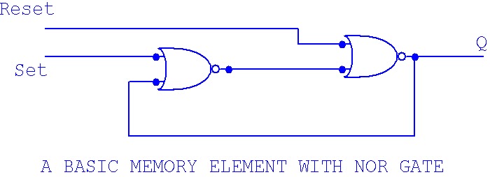
A memory element is referred to as a storage element. A basic memory element can formed using NAND or NOR gate. The above arrangement of NOR gate is a basic memory element that can withhold a logic. The arrangement below is a modified version which is also known as SR Latch.
Summarization of mentioned characteristic table for above SR latch is given below :
- When Q=0, Q'=1 and when Q=1,Q'=0 under normal conditions
- When R=0 and S=1, the latch is set into "S E T" state i-e Q=1 and Q'=0
- When R=1 and S=0, the latch is set into "R E S E T" state i-e Q=0 and Q'=1
- When both R and S equals low logic, the SR latch holds is previous states
- The last possibility of R=S=1 gives us the illegal (unpredictable|) value. Some authors say that Q=Q'=0 in this state.
More to Follow
09:39 |
Posted in
BASIC ELECTRONICS,
Digital Electronics,
SR Latch
|
Read More »
The above block-diagram shows a model of Ethernet automation. The same phenomenon is equally applicable for industrial Ethernet with some amendments. Also the above block diagram is point-point link approach only. The same can be extended to layer-2 network for more sophisticated automation.
What's happening in the block diagram? Touch Screen is placed at user end, say in a control room. Attached with it is a touch screen controller which get the coordinates of touch screen and pass over to Ethernet module. Ethernet module consists of a microcontroller, an Ethernet controller and Ethernet link. Microcontroller on the basis of received coordinates will pass the instructions to Ethernet Controller (ENC-28J60) over SPI. Ethernet controller will then transmit control words / data to its counterpart at the other end. Microcontroller will then drive the triac based or whatever the circuitry maybe accordingly.
More to follow!
11:19 |
Posted in
BASIC ELECTRONICS
|
Read More »

What is a Servo Motor? A servo motor comprises of mostly DC motors with feedback for position controlling. Stepper motor is also used for position controlling but without feedback. Mostly Servo Motors are DC because they provide high locking power. The above block diagram depicts the basic block diagram that most of the servo systems are based on. Microcontroller provides PWM signal to the H-Bridge which onwards drive the motor in either direction on the basis of received input PWM signal. Lets say if PWM signal of 50% duty cycle locks the motor, so increasing or decreasing PWM value will drive the motor in CW or CCW direction. The Shaft of the motor is connected to potentiometer thus changing the Vf ( Feedback Voltage) as the motor rotates. User can set the desired position of the motor using another potentio meter. This is the Set-point voltage. Microcontroller takes the difference of both the voltages i-e Feedback and Set-point and generates a PWM signal such that Motor reaches the desired position. When it does do, the difference gets zero and ultimately motor comes into locking position. This is how DC motor servo system operates. More to Follow!
13:08 |
Posted in
BASIC ELECTRONICS,
Block Diagrams,
How Stuff Works?
|
Read More »
Data Acquisition System is an important subject having its vast applications specially in industries. Often Data Acquisition System is abbreviated as DAS or DAQ. The process that most of the Data Acquisition System follows is to sample the data that represents real time conditions and to convert it in digital form that computers and processors can manipulate it.
The basic Block Diagram of DAS (Data Acquisition System) can be seen below :
Rights Reserved : http://elprojects.blogspot.com
The data from sensors is fed into ADC for mapping it to digital form. Typical ADC consists of a Sampler, a Quantizer and an encoder. The selection criterion of ADC is an other subject that needs another dedicated post. The data taken from ADC is then fed into microprocessor or microcontroller for the operations like memory or internet provision for remote accessing.
Few of the reasons for the emergence of DAS to digitally acquire data and for Analog Obsoleteness are as under:
- No processing can be done
- More memory needed
- Less readable due to Infinite Readings
12:58 |
Posted in
BASIC ELECTRONICS
|
Read More »
A number of Temperature Sensors / Heat Detectors are available in the market. Some of them includes:
All of the aforementioned have their own advantages and disadvantages. The pros and cons of each of the following are summarized below in a nutshell:
THERMISTOR:
This device offers the benefit of a very high sensitivity for a range of temperatures but has a non-linear scale. Extensive mathematical calculations are required to cater for this nonlinearity. The benefit is that it is very cheap compared to others. Normally used to detect a threshold temperature and used where accuracy is not needed.
THERMOCOUPLE:
The major advantage that a thermocouple offers to us is the Temperature range. It can be used for a very wide range of temperatures but at the same time it is highly insensitive. Dedicated linearize-rs like AD594( for J-Type - Temp range: 1800'C) and AD595 ( for K-Type - Temp range: 1200'C) are used compensation / amplification / linearization purposes.
DIODE AS TEMPERATURE SENSOR:
The diode is an extremely low cost device but has the disadvantage of a non-linear scale and rates poorly on the reliability scale.
RTD:
Resistor Temperature Device gives linear change in voltage with temperature. Famous of them are PT100 and PT1000. It also has a range that is suitable for normal laboratory and typical applications like fire alarm system. The cost of the RTD sensor is also less compared to thermocouple.
Solid State temperature sensor that gives linear response. Often there is no need to connect ADC. Range is also suitable for most applications. For more details see LM34/LM35/LM334/LM335 Selection Guide.
11:43 |
Posted in
BASIC ELECTRONICS,
How Stuff Works?
|
Read More »


